NVIDIA introduced a pivotal breakthrough in AI technology by unveiling its next-gen Blackwell-based GPUs at the NVIDIA GTC 2024.
As the AI and machine learning sectors continue to evolve at a breakneck pace, NVIDIA’s latest innovation, the Blackwell architecture, is set to redefine AI and HPC with unmatched parallel computing capabilities.
NVIDIA showcased a new set of technologies that promise to accelerate AI training and inference like never before. They unveiled the Blackwell GPUs, the GB200 Super Chip, and the GB200 NVL72. Each represents groundbreaking innovation.
In this article, we’ll break down NVIDIA’s Blackwell architecture. What does it represent for high-performance computing, and how does it improve the Hopper architecture? Then, we will unpack each of the new products.
Blackwell vs Hopper
The Blackwell architecture is named in honor of David Blackwell, the esteemed mathematician and statistician. Blackwell's groundbreaking work and contributions to game theory and statistics have left an indelible mark on the field, making his name synonymous with innovation and excellence in mathematical sciences. This homage reflects the new platform's groundbreaking nature and advanced computational capabilities.
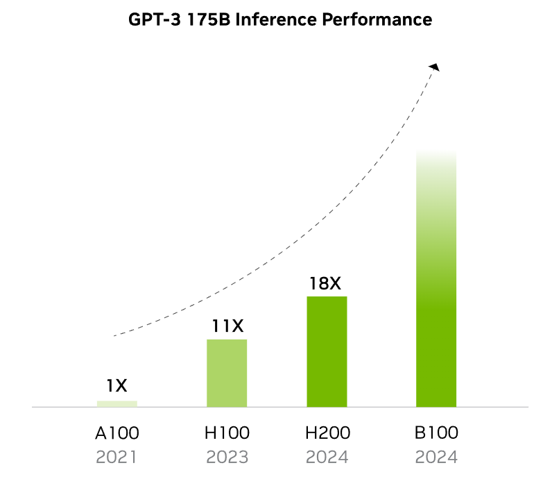
NVIDIA’s Blackwell architecture will have the largest chip yet, with 104 billion transistors. Blackwell GPUs (B100 & B200) adopt dual-chipset designs, representing a significant leap from Hopper. For instance, the B100 has 128 billion more transistors and five times the AI performance of the H100.
 Source: NVIDIA
NVIDIA’s Blackwell GPUs pack 208 billion transistors and are manufactured using a custom-built TSMC 4NP process. All Blackwell products feature two reticle-limited dies connected by a 10 terabytes per second (TB/s) chip-to-chip interconnect in a unified single GPU.
The Blackwell architecture offers improved performance with:
- FP8 Performance: The Blackwell architecture offers 20 PetaFLOPS (PFLOPS) of performance at FP8 precision, which is 2.5 times the performance of the Hopper architecture.
- FP6 Performance: Like FP8, FP6 performance on the Blackwell architecture is also 20 PFLOPS, a 2.5-time improvement over the Hopper architecture.
- FP4 Performance: This is a significant leap, with Blackwell offering 40 PFLOPS in the new FP4 metric, five times the performance of Hopper. This indicates a strong emphasis on improving performance for lower-precision computations, which are crucial for AI inference.
- HBM Model Size: NVIDIA’s Blackwell architecture supports models up to 740 billion parameters in size, which is six times larger than what Hopper architecture could manage. This massive increase supports the development and operation of larger and more complex AI models.
- HBM Bandwidth: The High-Bandwidth Memory (HBM) bandwidth on Blackwell is 34 Terabytes per parameter second (TB/s), which is five times the bandwidth available on Hopper. This allows for faster data transfer rates, which significantly improves computing performance.
- NVLink All-Reduce with SHARP: The Blackwell architecture offers 7.2 TB/s NVLink all-reduce capabilities with SHARP technology, four times the capability of Hopper architecture. SHARP (Scalable Hierarchical Aggregation and Reduction Protocol) enhances collective communication operations, which is crucial for distributed AI and machine learning tasks.
With the Blackwell architecture, NVIDIA introduces a fifth-generation NVLink, offering unprecedented levels of parallelism and bandwidth that considerably outpace the Hopper architecture’s capabilities. These advancements underscore Blackwell’s potential to power next-generation AI and high-performance computing applications.
The Blackwell architecture also comes with Secure AI. Secure AI protects your AI data even when they are being used. It increases security without reducing speed. This allows companies to safely work on even the most complex AI projects, protecting their ideas and enabling secure training, analysis, and information sharing between devices.
Blackwell also has intelligent resiliency with a dedicated Reliability, Availability, and Serviceability (RAS) Engine to identify potential faults that may occur early on to minimize downtime. Its RAS Engine provides in-depth diagnostic information to identify areas of concern and plan maintenance.
NVIDIA also introduced a comprehensive suite of products leveraging the Blackwell architecture to reshape the computational landscape. Here are some of them.
NVIDIA B100 and B200
NVIDIA is building on the Blackwell architecture by introducing two new GPUs, the B100 and B200. These GPUs feature a dual-die design, with each die containing four HBM3e memory stacks offering 24GB per stack and a bandwidth of 1 TB/s on a 1024-bit interface.
The B100 and B200 GPUs also improve the precision of floating-point operations. They come with a transformer engine that dynamically and automatically rescales and recasts numerical precision to a lower format whenever possible. This improves machine learning computations because when dealing with small floating-point numbers, the accuracy of the calculations affects the ability and accuracy of machine learning models.
CUDO Compute will offer the NVIDIA B100 as soon as it is released. Register your interest now to be the first in line to use the NVIDIA B100.
While NVIDIA did not explicitly provide the benchmarks for the B100 and the B200 GPUs, we have broken down their specifications based on theHGX specifications they released.
| SPECIFICATION | HGX B200 | HGX B100 |
|---|---|---|
| GPUs | HGX B200 8-GPU | HGX B100 8-GPU |
| Form factor | 8x NVIDIA B200 SXM | 8x NVIDIA B100 SXM |
| HPC and AI compute (FP64/TF32/FP16/FP8/FP4)* | 320TF/18PF/36PF/72PF/144PF | 240TF/14PF/28PF/56PF/112PF |
| Memory | Up to 1.5TB | Up to 1.5TB |
| NVIDIA NVLink | Fifth generation | Fifth generation |
| NVIDIA NVSwitch™ | Fourth generation | Fourth generation |
| NVSwitch GPU-to-GPU bandwidth | 1.8TB/s | 1.8TB/s |
| Total aggregate bandwidth | 14.4TB/s | 14.4TB/s |
Source: NVIDIA
NVIDIA B100
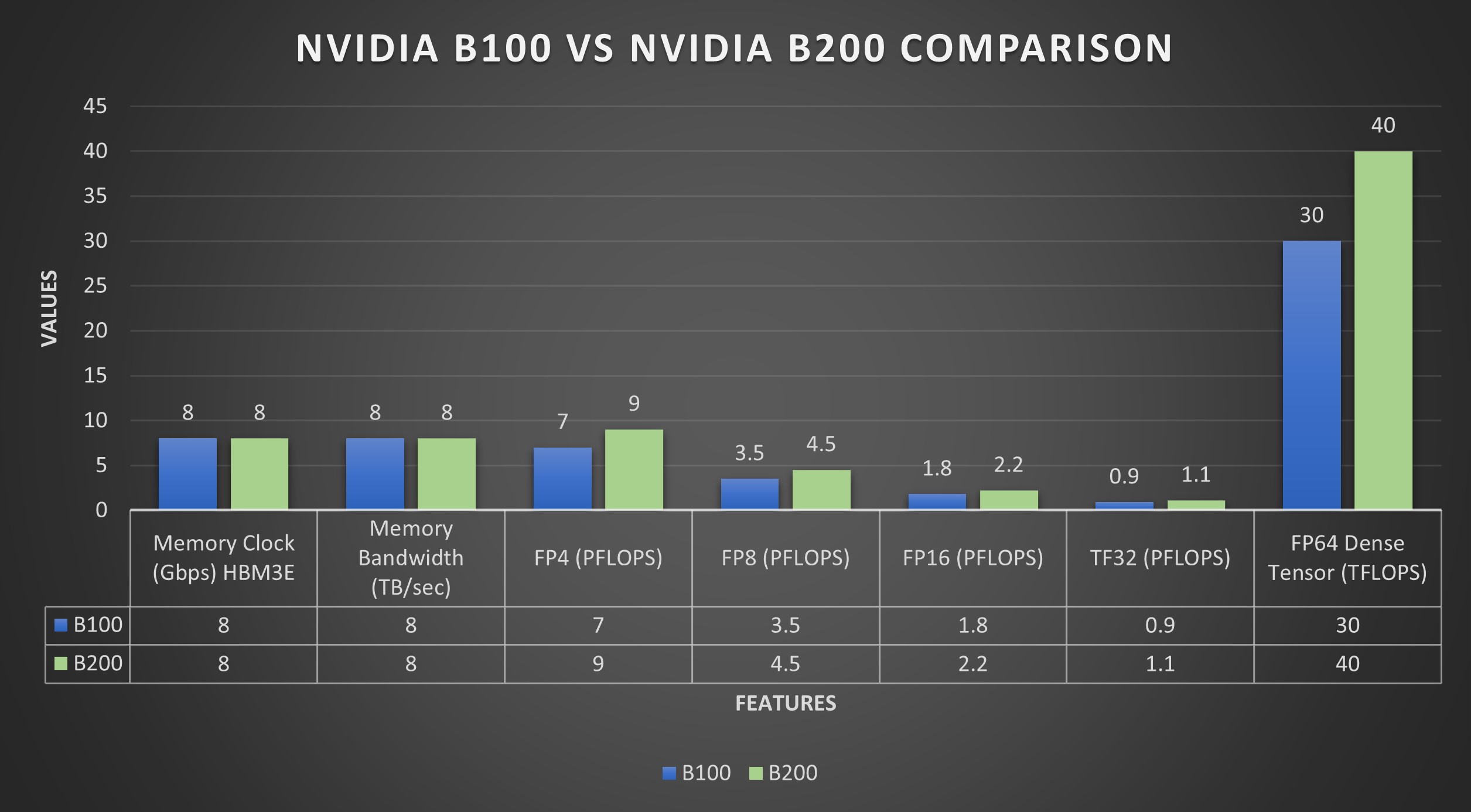
The B100 Blackwell GPU provides balanced computational efficiency. It delivers up to 7 PFLOPS for dense FP4 tensor operations, where 'dense' implies that most of the tensor's elements are non-zero, necessitating comprehensive computation. In contrast, it achieves up to 14 PFLOPS for sparse FP4 operations, where 'sparse' indicates that most elements are zero, allowing for optimized, faster processing due to fewer non-zero elements needing calculation.
For FP6/FP8 tensors, essential in balancing precision and computational speed, the B100 reaches 3.5/7 PFLOPS for dense/sparse tasks, respectively. Its INT8 tensor performance, critical for fast data inference, stands at 3.5/7 POPS for dense/sparse scenarios.
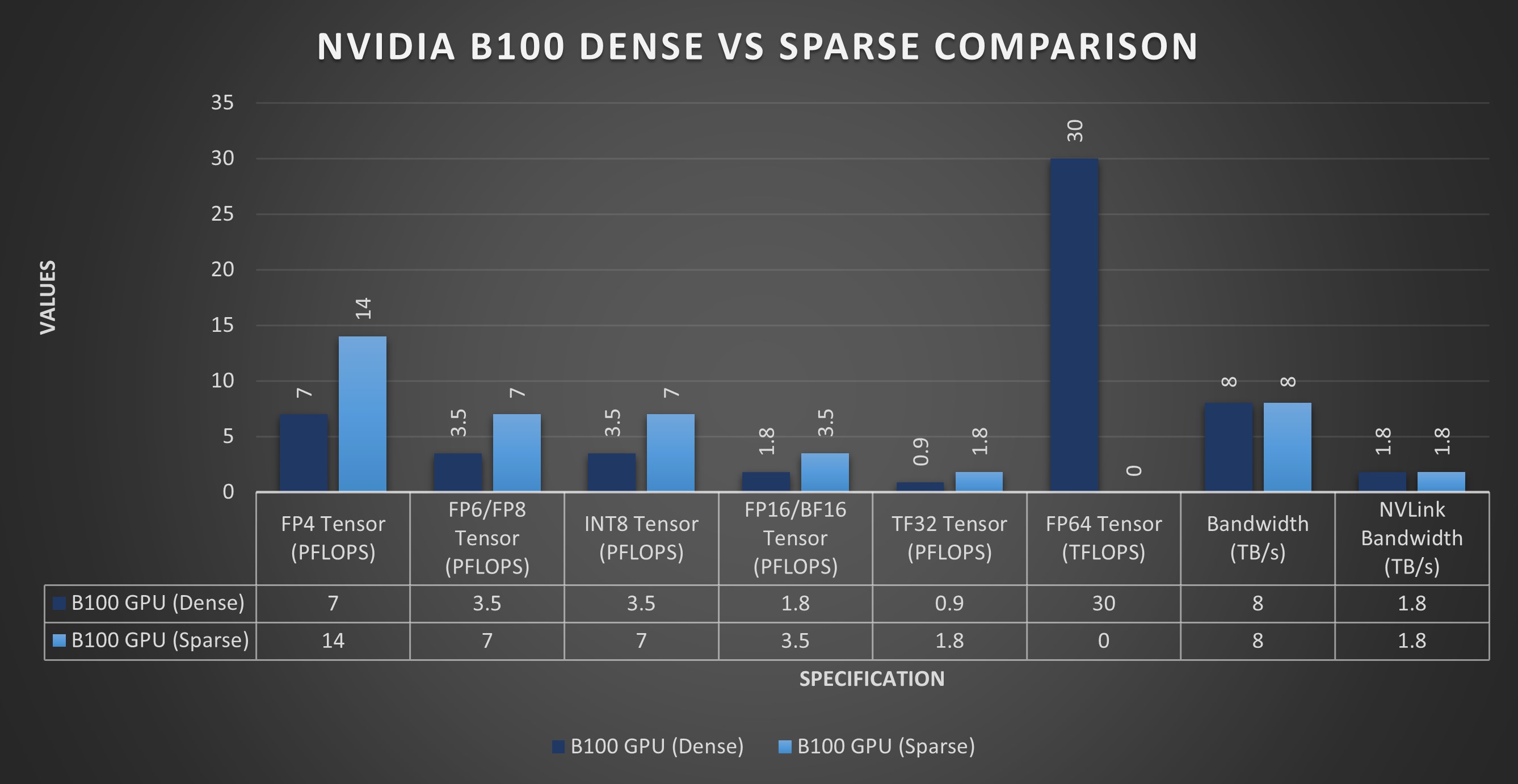
In higher accuracy requirements, the B100's FP16/BF16 tensors operate at 1.8/3.5 PFLOPS for dense/sparse, and TF32 tensors at 0.9/1.8 PFLOPS, supporting a range of precise computing tasks. Furthermore, it offers 30 TFLOPS in FP64 dense computations for scientific applications requiring the utmost accuracy.
The GPU has 192GB of memory, facilitating substantial data handling. It supports an 8 TB/s memory bandwidth and an equivalent 1.8 TB/s NVLink bandwidth for swift data communication. With a 700W power specification, the B100 stands out as an energy-efficient option for complex computational setups requiring balanced power and performance.
NVIDIA B200
The B200 Blackwell GPU achieves up to 9 PFLOPS in dense and 18 PFLOPS in sparse FP4 tensor operations. For FP6/FP8 tensor operations, balancing precision and speed, the B200 records 4.5/9 PFLOPS for dense/sparse activities, respectively. Its INT8 tensor capability, important for quick data analysis and inference, reaches 4.5/9 POPS for dense/sparse computations, ensuring efficient real-time processing.
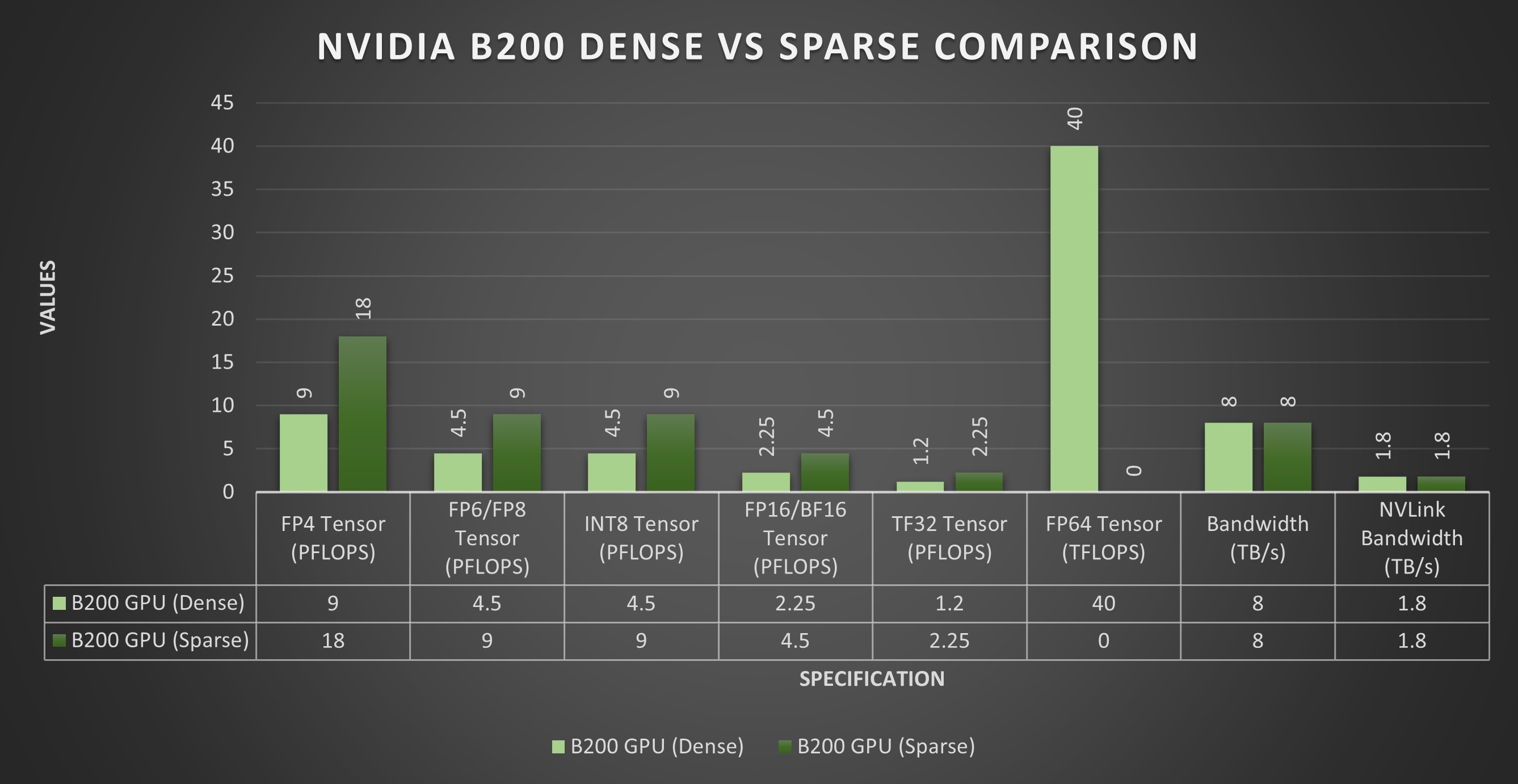
The B200 would shine in precision tasks with 2.25/4.5 PFLOPS for dense/sparse FP16/BF16 tensors and 1.2/2.25 PFLOPS for dense/sparse TF32 tensors, suitable for various scientific and machine learning applications. For ultimate precision, such as in detailed scientific calculations, it offers a solid 40 TFLOPS in FP64 dense computations.
| SPECIFICATION | B100 (Dense) | B100 (Sparse) | B200 (Dense) | B200 (Sparse) |
|---|---|---|---|---|
| Configuration | Blackwell GPU | Blackwell GPU | Blackwell GPU | Blackwell GPU |
| FP4 Tensor | 7 PFLOPS | 14 PFLOPS | 9 PFLOPS | 18 PFLOPS |
| FP6/FP8 Tensor | 3.5 PFLOPS | 7 PFLOPS | 4.5 PFLOPS | 9 PFLOPS |
| INT8 Tensor | 3.5 POPS | 7 POPS | 4.5 POPS | 9 POPS |
| FP16/BF16 Tensor | 1.8 PFLOPS | 3.5 PFLOPS | 2.25 PFLOPS | 4.5 PFLOPS |
| TF32 Tensor | 0.9 PFLOPS | 1.8 PFLOPS | 1.2 PFLOPS | 2.25 PFLOPS |
| FP64 Tensor | 30 TFLOPS | - | 40 TFLOPS | - |
| Memory | 192GB (8x24GB) | 192GB (8x24GB) | 192GB (8x24GB) | 192GB (8x24GB) |
| Bandwidth | 8 TB/s | 8 TB/s | 8 TB/s | 8 TB/s |
| NVLink Bandwidth | 1.8 TB/s | 1.8 TB/s | 1.8 TB/s | 1.8 TB/s |
| TDW | 700W | 700W | 1000W | 1000W |
Equipped with 192GB of memory, the B200 enhances large-scale data processing. It is supported by an 8 TB/s memory bandwidth and a corresponding 1.8 TB/s NVLink bandwidth, facilitating fast and efficient data transfer. With a power consumption rated at 1000W, the B200 is designed for energy efficiency in demanding computational environments, balancing high-end performance and power usage.
GB200 and GB200 NVL72
NVIDIA also unveiled the GB200 Grace Blackwell Superchip. It combines two NVIDIA B200 Tensor Core GPUs with an NVIDIA Grace CPU over a 900GB/s ultra-low-power NVLink chip-to-chip interconnect.
The Grace Blackwell Superchip's chip-to-chip link is completely memory-coherent, creating a unified chip without memory localization. The Superchip utilizes HBM3e memory, providing up to 384 GB with a bandwidth of 16 TB/s, facilitating rapid data handling.
It includes a decompression engine and multimedia decoders and is built on 72 ARM Neoverse V2 cores with various cache levels (L1, L2, and L3 caches) for optimized data retrieval speed. It integrates the latest NVLink 5.0 and PCIe Gen 6, supporting high-speed data transfers.
| SPECIFICATION | GB200 NVL72 | GB200 Grace Blackwell Superchip |
|---|---|---|
| Configuration | 36 Grace CPU: 72 Blackwell GPUs | 1 Grace CPU: 2 Blackwell GPU |
| FP4 Tensor Core | 1,440 PFLOPS | 40 PFLOPS |
| FP8/FP6 Tensor Core | 720 PFLOPS | 20 PFLOPS |
| INT8 Tensor Core | 720 POPS | 20 POPS |
| FP16/BF16 Tensor Core | 360 PFLOPS | 10 PFLOPS |
| TF32 Tensor Core | 180 PFLOPS | 5 PFLOPS |
| FP64 Tensor Core | 3,240 TFLOPS | 90 TFLOPS |
| GPU Memory | Bandwidth | Up to 13.5 TB HBM3e | 576 TB/s | Up to 384 GB HBM3e | 16 TB/s |
| NVLink Bandwidth | 130TB/s | 3.6TB/s |
| CPU Core Count | 2,592 Arm® Neoverse V2 cores | 72 Arm Neoverse V2 cores |
| CPU Memory | Bandwidth | Up to 17 TB LPDDR5X | Up to 18.4 TB/s | Up to 480GB LPDDR5X | Up to 512 GB/s |
The Grace Blackwell Superchip which is designed for scalability, supports Multi-Instance GPU capabilities and is packaged for easy server integration. The TDP is configurable up to 2700 W, allowing energy management according to computational needs.
In practical applications, the GB200 significantly improves computational tasks such as database processing, with an 18-times speed increase over traditional CPUs, reducing energy use and total cost of ownership. It accelerates physics-based simulations crucial for product design, allowing for cost-effective digital testing. For ASIC design, exemplified by the Cadence SpectreX simulator, it offers a 13-times speed improvement. Additionally, in computational fluid dynamics, the GB200 increases simulation speeds by up to 22 times, enhancing efficiency in engineering and design.
The GB200 NVL72 combines 36 Grace CPUs and 72 Blackwell GPUs. It is a liquid-cooled, rack-scale 72-GPU NVLink domain that can act as a single massive GPU. It introduces cutting-edge capabilities and a second-generation Transformer Engine that significantly accelerates LLM inference workloads, enabling real-time performance for resource-intensive applications like trillion-parameter language models.
Inference is one of the key aspects of generative AIs and LLMs. It refers to the phase where the model, after being trained, generates or predicts new data points (tokens) based on the input it receives. This process is referred to as "token generation."
 Source: NVIDIA GTC
Thanks to the FP4, tensor core, transformer engine, and NVLink switch, GB200 NVL72 can generate 30 times more tokens than Hopper, enabling 1.8 TB/s of GPU-to-GPU interconnect.
The GB200 NVL72 is designed for high-level computing tasks and requires advanced networking to function optimally. This is facilitated by integrating NVIDIA Quantum-X800 InfiniBand, Spectrum-X800 Ethernet, and BlueField-3 DPUs, which enhance the performance, efficiency, and security of large-scale AI data centers.
Quantum-X800 InfiniBand is essential for constructing the AI compute framework, enabling connections for over 10,000 GPU units in a two-level fat-tree topology. This setup significantly improves, being five times more capable than the previous Quantum-2 generation from NVIDIA.
In parallel, the NVIDIA Spectrum-X800 and BlueField-3 DPU platforms are implemented to extend capabilities across the data center. They provide fast GPU access to data, ensure secure environments for multiple users (multi-tenancy), and facilitate streamlined data center operations. This combination supports the GB200's role in processing extensive AI data sets efficiently.
Blackwell’s practical benefits for generative AI
NVIDIA's Blackwell architecture is designed to accelerate generative AI, significantly reducing training and inference times for faster research and product development across the tech industry. From a practical implication point of view, this translates into the ability to address previously computationally expensive problems like the high-fidelity climate simulations undertaken by Earth-2.
With the introduction of FP4, the accuracy loss when training generative AI is minimal. FP4 also increases speed and accuracy by allowing models to be trained for longer durations within the same timeframe.
Blackwell-based GPUs can be used to create highly detailed virtual realities, which can help accelerate the training of multimodal LLMs and robots with more nuance and better context. According to this comprehensive LinkedIn post, A forthcoming UC Berkeley study will demonstrate how generative AI training on NVIDIA's Blackwell platform can lead to a 30% boost in robots' ability to complete tasks in real-world settings.
In addition, NVIDIA’s B100 and B200 GPUs can facilitate advancements in complex fields from materials science to medicine, even self-driving cars. Their capabilities will allow for tackling previously unapproachable challenges, driving forward innovation and efficiency in various industries.
CUDO provides the opportunity to be first in line to rent NVIDIA’s latest B100 GPUs. In the meantime, you can access CUDO’s A100, H100, or H200 GPUs and then be first in line for a cloud upgrade to the latest GPU hardware.
Register to reserve access today.
Learn more about CUDO Compute: Website, LinkedIn, Twitter, YouTube, Get in touch.
Continue reading
Everything You Need to Know About the NVIDIA A40: Price, Specification, Performance, and More
13 min read
NVIDIA H100 vs H200: How Will They Compare?
10 min read
PyTorch vs Tensorflow: Comparative Analysis of AI Frameworks
13 min read
CUDO Compute Boosts GPU Fleet: More NVIDIA A40s, A6000s and V100s Now Available to Power AI and HPC Globally
3 min read